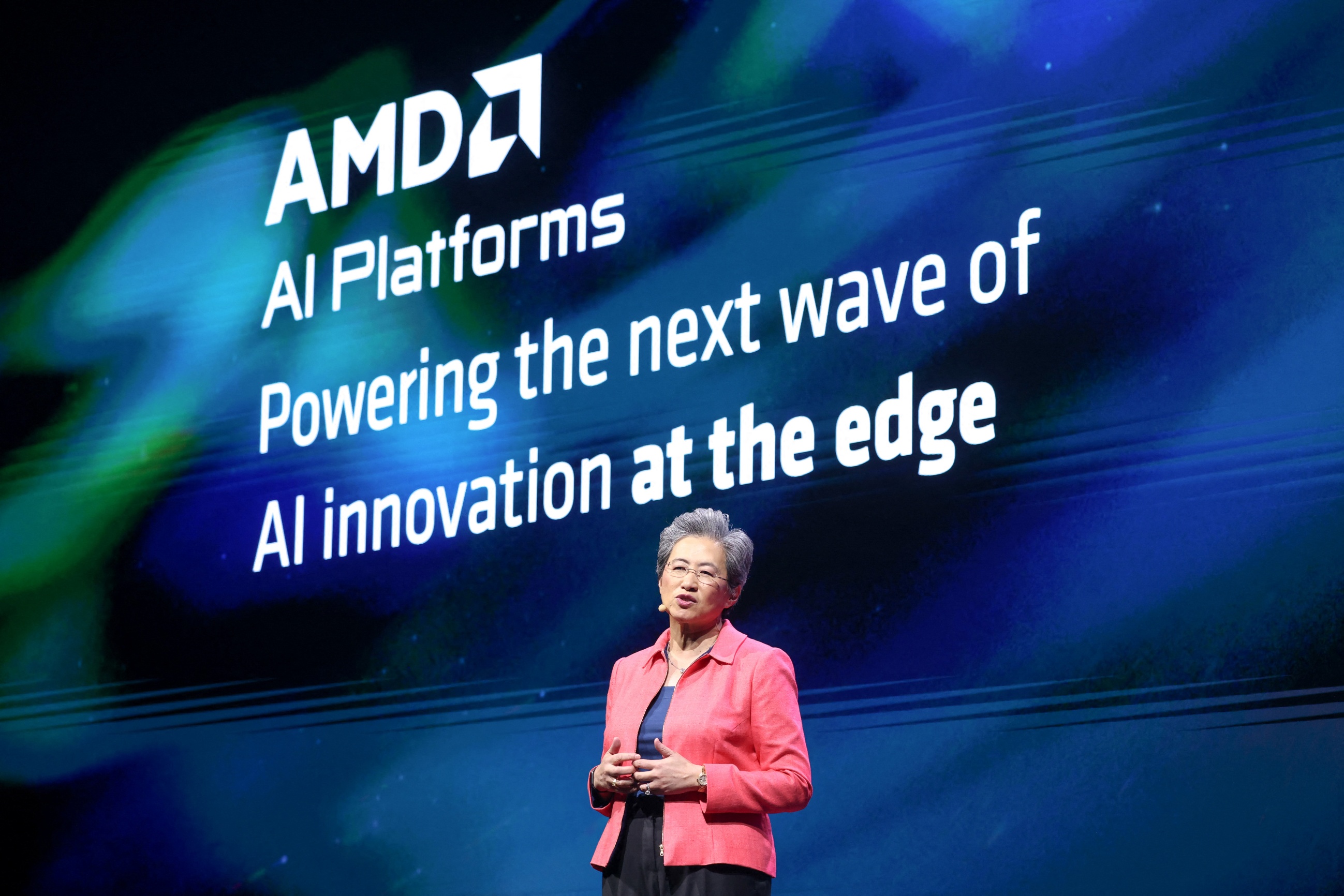
AMD's Advancing AI 2026 opened at Moscone West in San Francisco on July 22, 2026 with the commercial debut of EPYC "Venice" — the first x86 server processor in the industry to enter volume production on TSMC's 2-nanometer N2 process — alongside the Instinct MI455X GPU accelerator and a rack-scale AI system called Helios that ties them together. Meta, Microsoft, Oracle and OpenAI have already committed capacity, giving AMD a full current-generation AI stack in market roughly 12 months ahead of Intel's next-generation P-core Xeon "Diamond Rapids" response.
EPYC Venice: 256 Zen 6 Cores On TSMC N2
Venice is the first HPC-scale chip anywhere in the industry to run in sustained production on TSMC N2, which replaces the FinFET transistor geometry that has dominated since 2011 with gate-all-around (GAA) nanosheet transistors. TSMC's own characterization places the N2 benefit at 10-15% higher performance at equivalent power over N3E, or 25-30% lower power at equivalent performance. AMD used the extra headroom to redesign the socket: eight CCDs of 32 Zen 6c cores each, dual slender I/O dies on 4nm silicon, 16 DDR5 channels delivering up to 1.6 TB/s of memory bandwidth per socket (versus roughly 614 GB/s on Turin), and PCIe Gen 6 — collectively giving the CPU enough throughput to actually feed a Helios rack of MI455X GPUs.
Helios: 72 MI455X GPUs, 31 TB Of HBM4
Each Instinct MI455X carries 432 GB of HBM4 and 19.6 TB/s of memory bandwidth. Helios assembles 72 MI455X GPUs in a double-wide rack alongside Venice CPUs and Pensando Vulcano 800G NICs, delivering 31 TB of aggregate HBM4 — enough to hold a multi-hundred-billion-parameter model plus inference cache on a single rack without tensor parallelism. AMD rates the rack at 2.9 exaFLOPS FP4 inference and 1.4 exaFLOPS FP8 training in roughly 140 kW, versus 190-230 kW for NVIDIA's Vera Rubin NVL72. NVIDIA still leads on aggregate compute — 3.6 exaFLOPS FP4 for Vera Rubin — but Helios's structural advantage is memory capacity: 31 TB HBM4 against roughly 20.7 TB.

The UALink Open-Standard Bet
Helios's GPU-to-GPU fabric runs on UALink — the open interconnect standard AMD, Microsoft, Broadcom, Cisco, Google, HPE, Intel and Meta co-founded in May 2024, and which now has more than 85 member companies. Initial H2 2026 systems use UALink-over-Ethernet with a Broadcom co-designed switch fabric because purpose-built UALink switching silicon from Astera Labs and others is not production-ready until 2027. Aggregate intra-rack scale-up bandwidth is 260 TB/s, on paper comparable to NVIDIA's NVLink72 at 259 TB/s. Microsoft's July 20 Azure Helios commitment — the ND MI455X v7 for inference, an HDv2 EPYC Venice instance for agentic AI, and HXv2 for EDA — is the validation event the UALink Consortium was designed to produce.
Supply, ROCm, And What Enterprise Buyers Actually Get
All 2026 HBM4 production is allocated to hyperscale customers, with independent analysis placing MI455X mass production at Q2 2027. Enterprise buyers outside Meta, Microsoft, Oracle and OpenAI should plan Helios procurement in 2027, or reach the hardware indirectly through Oracle's 50,000-GPU MI450 supercluster launching in Q3 2026. Standalone Venice CPU systems ship earlier, in Q3 2026, on the new SP7 socket — physically incompatible with SP5 Turin infrastructure, so buyers plan a full platform swap. On software, ROCm 7.2.4 lands as a first-class PyTorch 2.7.0 backend at roughly 90-95% of NVIDIA H100 throughput on standard LLM inference, at 15-30% lower cost. The gap widens for training (20-30% ROCm deficit) and CUDA-kernel-dependent pipelines. Dr. Lisa Su's keynote on July 23 is expected to close outstanding questions on Helios timelines and the MI500-series roadmap, extending the momentum from NVIDIA's own Japan supercomputer wins and Wistron's AI-server capacity build-out.
Reporting based on coverage from Tech Times, Videocardz, TechPowerUp, Tom's Hardware and AMD Investor Relations.