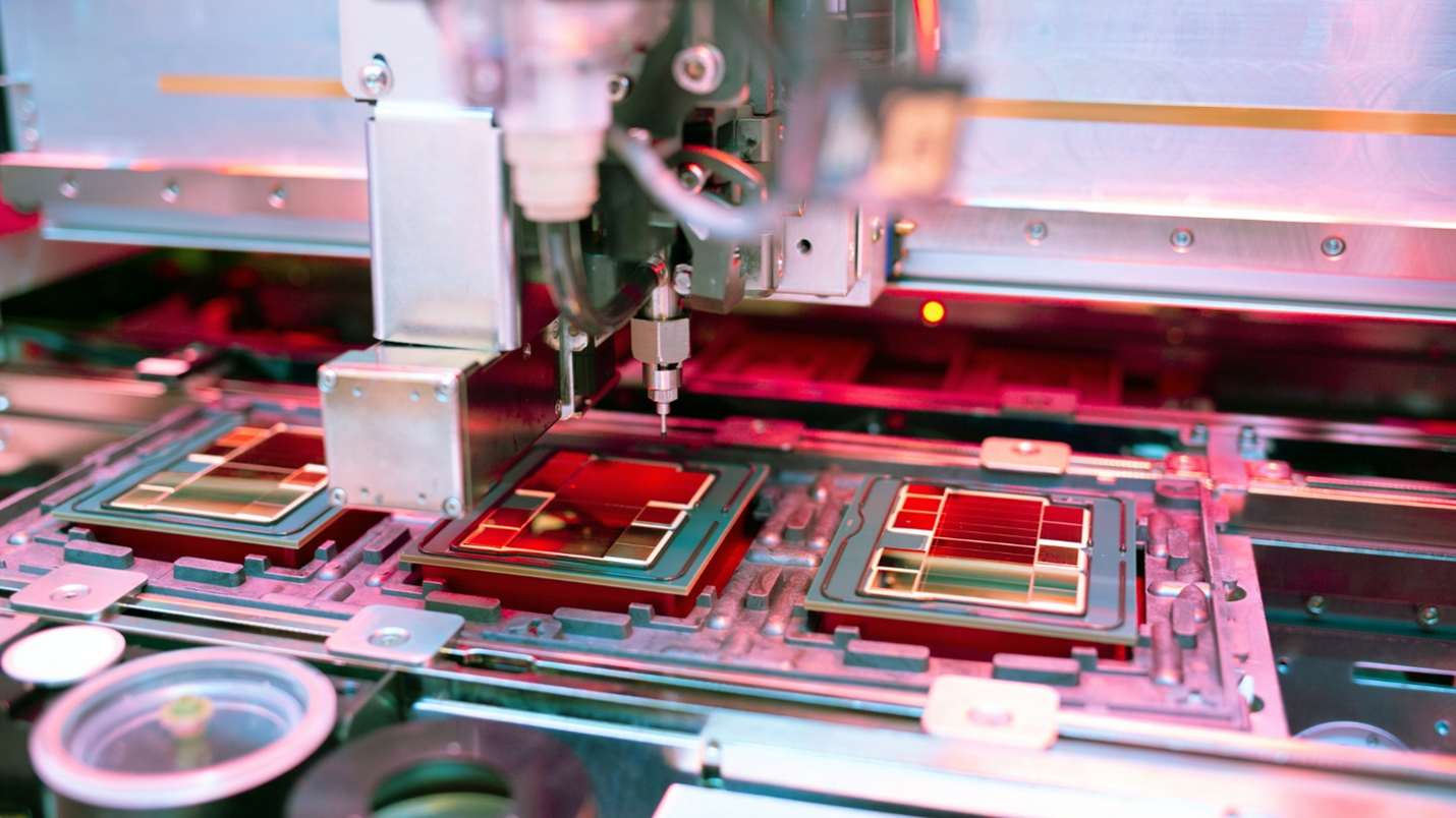
TSMC has begun engineering a new advanced chip-packaging platform that borrows from Intel's Embedded Multi-die Interconnect Bridge (EMIB), the world's largest foundry admitted this week. The program — referred to internally as "EMIB-like" — is being co-developed with Taiwan-based substrate maker Kinsus Interconnect Technology, and is designed to relieve the crushing capacity shortage in TSMC's dominant CoWoS packaging.
Why CoWoS Is No Longer Enough
For nearly a decade, TSMC's Chip-on-Wafer-on-Substrate (CoWoS) has been the industry standard for stitching GPU dies together with High-Bandwidth Memory stacks. But CoWoS is now completely sold out through 2026 and into 2027, with lead times of 52 to 78 weeks. TSMC is scaling from around 35,000 CoWoS wafer starts per month in late 2024 to a projected 130,000 by end-2026 — and it still cannot fill every order.
At the July 16 earnings call, TSMC CEO C.C. Wei acknowledged that packaging capacity is now the constraint on customer growth. The EMIB-like program with Kinsus is one answer.
How Intel's Approach Wins At Large Package Sizes
EMIB embeds small silicon bridges directly into the organic substrate, only where two chiplets need dense die-to-die connectivity. That avoids the giant single-piece silicon interposer that dominates CoWoS-S — a component that scales in cost with package size and now represents an estimated 40-60% of the total CoWoS bill of materials. Intel's EMIB currently supports packages exceeding 8x the reticle limit, with a 2028 target of more than 12x. TSMC's CoWoS-S sits around 3.3x today, with 5.5x on its near-term roadmap.
For inference-class ASICs and chiplet-heavy AI accelerators — designs from Google, Amazon and MediaTek that combine dies from multiple foundries — that architectural gap has become a live commercial threat.

Kinsus Steps Up From Supplier To Partner
Kinsus has been a Taiwan substrate incumbent for two decades, best known for BGA, flip-chip and ABF substrates supplied to the broader semiconductor assembly ecosystem. The TSMC deal repositions the Taoyuan-based company as a co-development partner, responsible for designing, testing and manufacturing the advanced substrates that house the embedded silicon bridges. Analysts already track a Kinsus expansion cadence of a new plant every two to three years — consistent with scaling a new packaging platform toward volume.
Markets React, Both Winners
Both stocks jumped on the news: TSMC's ADRs rose about 7% and Intel's shares surged more than 13%. The dual rally reflects a bigger point — the AI packaging market is expanding fast enough that TSMC's move validates Intel's approach without cannibalizing its own core business. Advanced packaging is projected by Yole Group to reach roughly $69.5 billion by 2029.
Intel's EMIB has been racking up wins: Google has booked more than 3 million TPUs on Intel packaging for 2028, AWS Trainium 3 is targeting EMIB-T, MediaTek is running a dual TSMC/Intel packaging strategy, and Nvidia is reportedly evaluating EMIB for its 2028 Feynman GPU. See our coverage on the Samsung-Broadcom $200B chip pact and Samsung's Q2 2026 HBM4 record for the broader HBM and foundry backdrop.
What Comes Next: CoPoS And Panel-Level Packaging
The EMIB-like program is not TSMC's only response. The company continues to advance CoPoS — Chip-on-Panel-on-Substrate — which builds packages on rectangular 310mm x 310mm panels instead of round wafers, enabling far larger assemblies. Morgan Stanley now projects CoPoS could hit mass production as early as 2028. Intel's own EMIB roadmap points to panel-level packaging that could accommodate 50x reticle-area packages within a similar horizon.
For now, the story is TSMC's engineers naming a program after their rival's technology — and markets reading the move as urgency, not weakness.
Reporting based on coverage from The Information, TechTimes, Wccftech and Tom's Hardware.