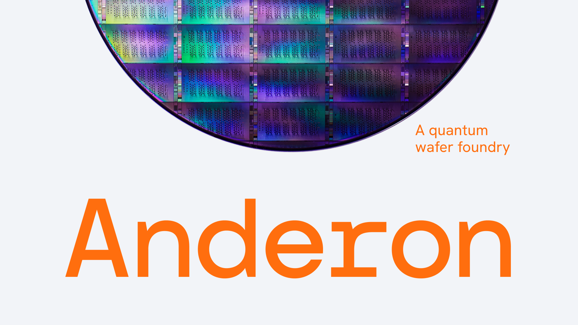
Anderon, the IBM-owned quantum wafer foundry, on September 16, 2026 finalized a $1 billion CHIPS and Science Act award from the U.S. Department of Commerce — locking in federal support for the country's first purpose-built pure-play quantum manufacturing site in Albany, New York.
A $2 Billion Total Bet
The Commerce agreement covers $1 billion in federal funding under the CHIPS Act, matched by another $1 billion of direct IBM investment. Together the pledges anchor an R&D acceleration program at the Albany NanoTech Complex to scale 300 mm wafer manufacturing for superconducting-qubit arrays, quantum I/O signaling and readout chains. The deal follows a letter of intent signed in May 2026.
First Wafers Already Running
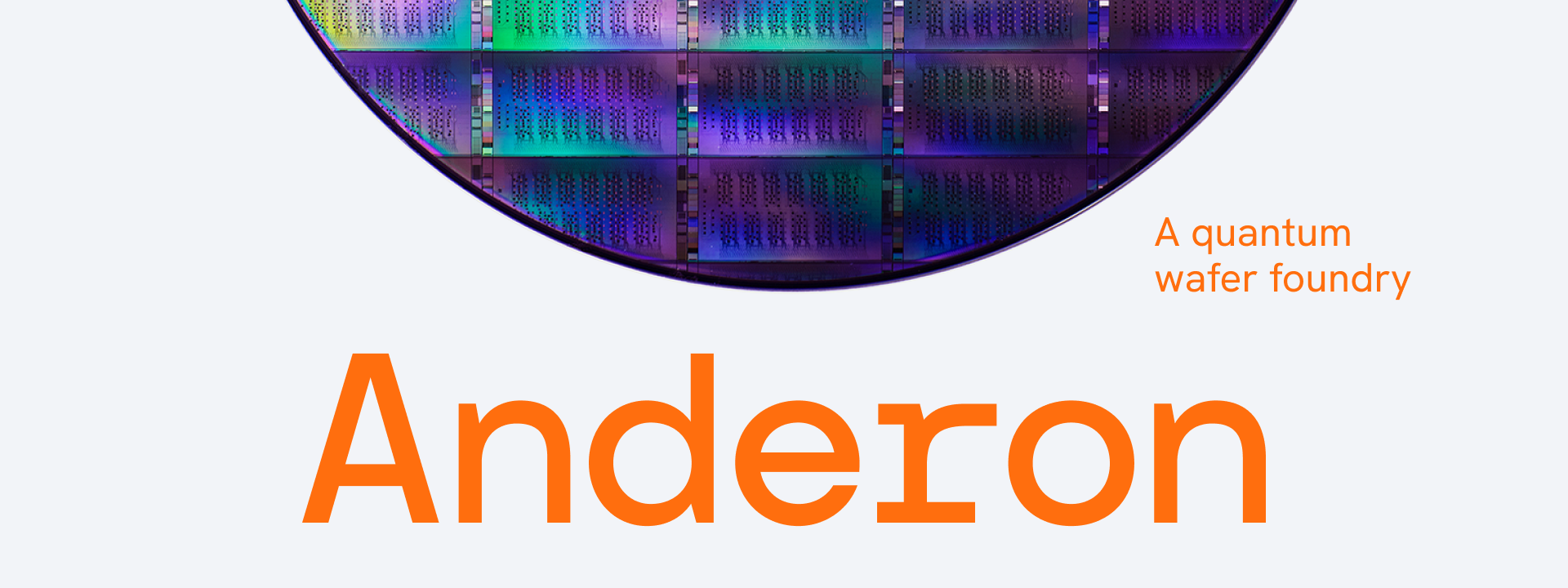
Anderon says initial production is under way, with first quantum wafers already through the foundry. The company was set up to extend IBM's Yorktown-based quantum roadmap — anchored by the Nighthawk processor and the forthcoming Starling error-corrected system — with dedicated volume manufacturing that also serves outside quantum builders.
Quotes
"This agreement strengthens our ability to deliver the manufacturing scale the quantum industry needs," said Anderon CEO Mukesh Khare. IBM Research Director Jay Gambetta added: "Anderon's focus on wafer fabrication gives us exactly that and strengthens our ability to execute."
Why It Matters
Superconducting qubits still require exquisitely uniform Josephson junctions and low-loss wiring — problems solved today only by a handful of R&D lines. Standing up a dedicated 300 mm pure-play foundry aims to break the throughput bottleneck that has capped fault-tolerant machine roadmaps. It also mirrors moves elsewhere: Novo Nordisk Foundation's 5,300 m² Copenhagen quantum chip fab, IQM's first on-prem system in Brazil, and IBM's own $1.2B acquisition of HRL Laboratories to fold silicon-spin qubits into the same fab.
Reporting based on coverage from IBM Newsroom, HPCwire and The Quantum Insider.