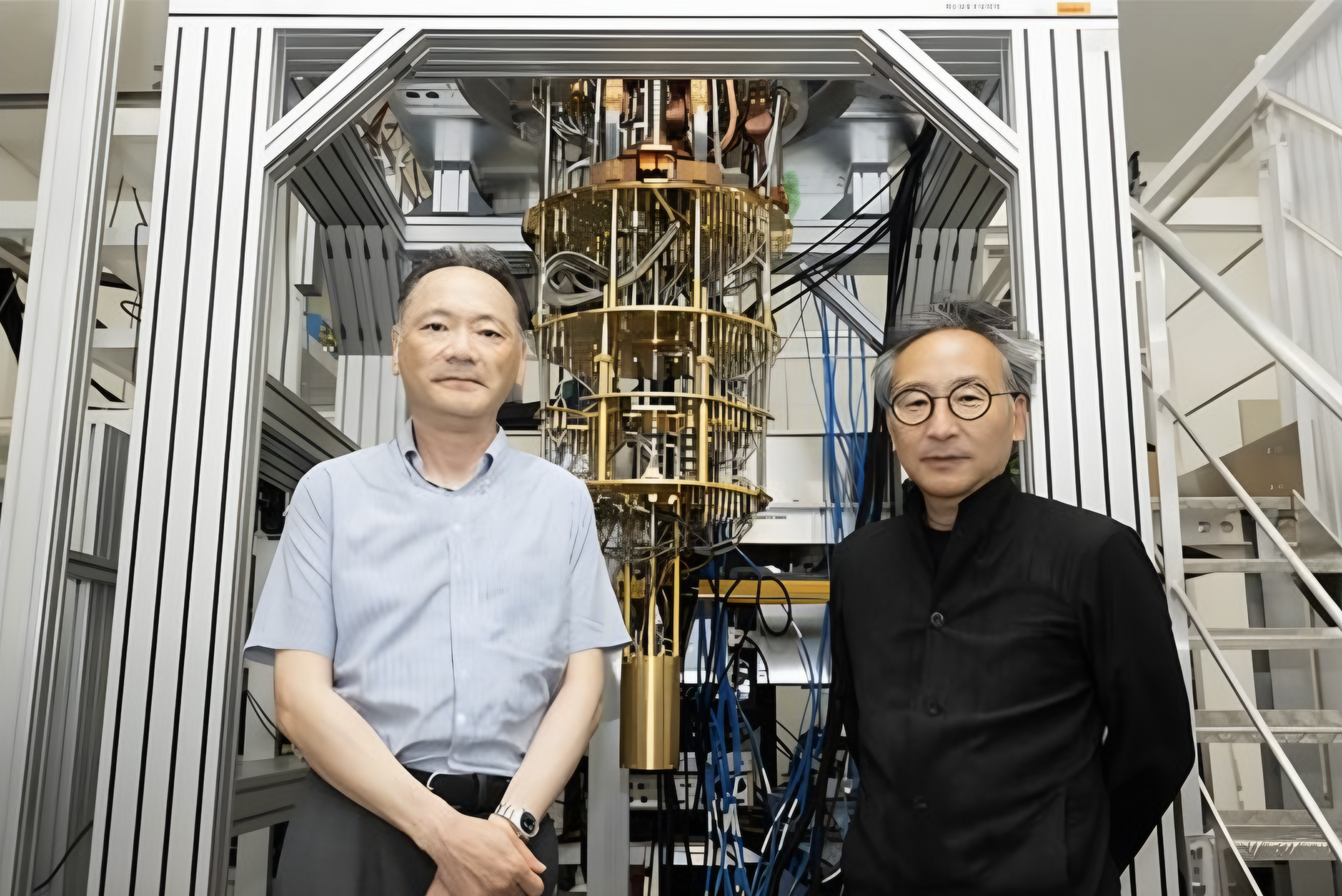
Hitachi announced on July 22, 2026 that it has been selected by Japan’s New Energy and Industrial Technology Development Organization (NEDO) to lead a national silicon-quantum computing R&D project alongside Intel K.K. and the National Institute of Advanced Industrial Science and Technology (AIST). The program will fabricate silicon spin-qubit processors on Intel’s 18A semiconductor node — one of the most advanced high-volume manufacturing processes in the world — and runs through March 2029.
Why Silicon Spin Qubits On Intel 18A
Silicon spin qubits store quantum information in the spin state of a single electron trapped in a nanoscale quantum dot. Unlike superconducting qubits, they are compatible with commercial CMOS lithography — the same EUV, ion implantation and gate-stack steps already running in Intel’s fabs. Intel 18A adds RibbonFET gate-all-around transistors and PowerVia backside power delivery, both of which improve gate uniformity and free front-side routing needed for dense qubit addressing.
Four Workstreams To 1,000 Qubits
The program is organized around four interlocking pillars: (1) co-development of industrial-scale 100-qubit chip architectures with peripheral cryogenic packaging and control electronics; (2) an open silicon-quantum process design kit (PDK) on Intel 18A, intended to let outside labs and startups design qubit hardware for industrial fabs the way classical chip designers already do; (3) 3D packaging technology for 1,000-qubit systems that survives the millikelvin wiring bottleneck; and (4) cloud access through AIST’s ~¥62 billion G-QuAT facility.
Milestone Timeline
Hitachi’s roadmap targets an initial cloud service via G-QuAT in fiscal 2027, a 100-qubit prototype capable of running quantum error-correcting codes by fiscal 2028, and a 3D-integrated 1,000-qubit platform by fiscal 2030. Those figures are research-scale, not fault-tolerant: reaching commercially useful fault tolerance is expected to demand roughly one million physical qubits, per current surface-code estimates.
The Consolidating Silicon-Spin Race
The July 22 announcement lands as competition tightens. IBM said on July 23 that it would acquire silicon-spin leader HRL Laboratories; GlobalFoundries stood up a quantum foundry unit in May; France’s Quobly is fabricating silicon spin qubits on STMicroelectronics’ FD-SOI line and joins OVHcloud’s sovereign cloud later in 2026. It also arrives as Infleqtion deploys neutral-atom hardware at the Illinois Quantum Park and PsiQuantum expands its DARPA Benchmarking work. What the Japanese consortium is banking on — an open PDK plus a leading-edge foundry — is the same ecosystem play that turned classical chip design into a global activity.
Reporting based on coverage from Hitachi, HPCwire, Tech Times, The Quantum Insider and Quantum Computing Report.