NVIDIA and TSMC have announced an expanded partnership to apply accelerated computing and AI across the full semiconductor design and manufacturing lifecycle, the companies said in a joint statement coinciding with NVIDIA CEO Jensen Huang’s annual Taipei industry dinner.
From CAD to wafer
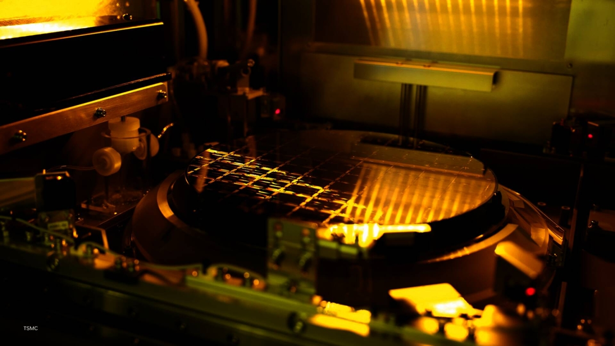
Under the agreement, TSMC will deploy NVIDIA’s cuLitho computational lithography stack, Omniverse digital-twin tooling and CUDA-X libraries across advanced fabs, with the stated goals of improving turnaround time, energy efficiency, yield and operational productivity. NVIDIA describes the deployment as the largest production rollout of cuLitho to date.
Why fabs need AI now
Each successive process node makes the physics of patterning, etching and inspection more punishing. Computational lithography corrects optical proximity effects in real time using physics-based simulation; running those simulations on GPUs rather than legacy CPU farms can compress mask-generation cycles from weeks to days while improving fidelity.
Anchoring the Taiwan supply chain
The announcement is part of a broader trip in which Huang reaffirmed Taiwan’s central role in NVIDIA’s supply chain, downplayed concerns over a competing “Tau Scaling Law” promoted by Huawei, and praised TSMC’s decade-long investment in advanced packaging. The Taiwanese government has announced 5.2 GW of new natural-gas generation by year-end to support the island’s ballooning fab power demand.

What changes for customers
For NVIDIA’s hyperscaler and merchant silicon customers, the partnership is meant to translate into faster ramps of new node families and tighter yield curves. The companies’ joint roadmap includes broader use of Omniverse digital twins for fab planning, complementing earlier work disclosed at Computex/GTC Taipei 2026 and the Cadence–NVIDIA physical AI alliance.
Reporting based on coverage from StockTitan and NVIDIA newsroom.