Chinese memory maker YMTC has climbed to third place globally in NAND bit shipments in Q2 2026 with a 14% share, according to Counterpoint Research data published on August 12, edging past Kioxia and closing on the SK hynix group. The move comes as YMTC ramps its Xtacking 4.0 architecture into mass production of 267-layer 3D NAND and readies fresh fab capacity that could take total design ceiling to 500,000 wafers per month.
Third In Bits, Fifth In Revenue
Counterpoint's Q2 chart shows Samsung leading with 25%, the combined SK hynix group at 22% (SK hynix 13% plus Solidigm 9%), and YMTC and Kioxia both rounded to 14%. Micron sits at 13% and SanDisk at 11%. But YMTC still ranks only fifth in NAND revenue: its mix is heavy in relatively low-priced consumer NAND, and the high-priced enterprise SSD (eSSD) tier where AI servers now buy — 48% of Q2 bit shipments, up from 26% a year ago — remains dominated by Samsung, SK hynix's Solidigm arm, Micron and Kioxia.
Xtacking 4.0 And The 267-Layer Push
YMTC's technical edge is Xtacking, its wafer-to-wafer bonding architecture that puts periphery/logic and memory-cell wafers on separate dies and bonds them together. Xtacking 4.0 adds copper-to-copper bonding with sub-micron alignment to cut signal paths, shrink die thickness and lift bandwidth. Counterpoint says YMTC is mass-producing 267-layer TLC 3D NAND — putting it within striking distance of Micron's 276-layer devices and Samsung and Kioxia/SanDisk's 286-layer parts — and developing 300+ layer NAND on the same platform.
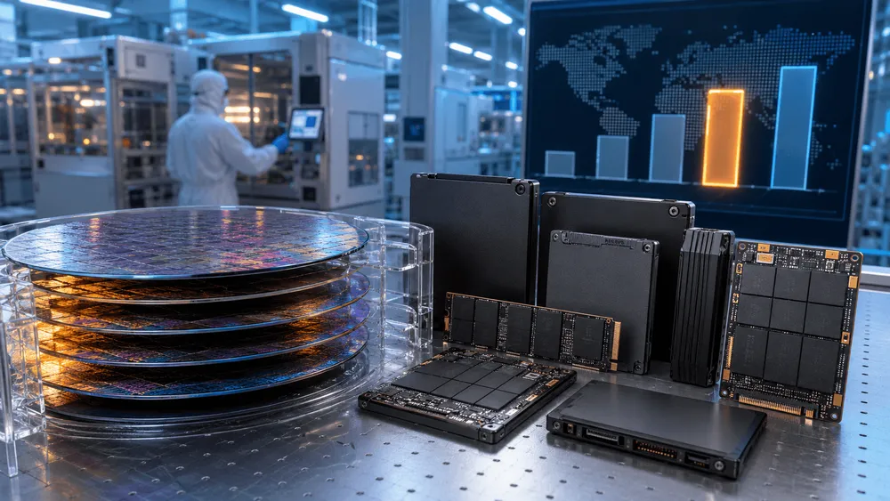
Fab Buildout Aims At 500K Wafers/Month
Reuters has reported that YMTC's two existing Wuhan fabs currently produce a combined 200,000 wafers per month, with a third fab in Wuhan now installing equipment and expected to ramp toward 50,000 wafers/month by 2027. Two additional fabs at undetermined locations are planned, each designed for 100,000 wafers/month at full operation — taking the design ceiling to roughly 500,000 wafers/month if all plans materialize. Sources told Reuters that more than 50% of the third fab's equipment was procured from Chinese suppliers, a workaround necessitated by U.S. export controls that added YMTC to the Entity List in December 2022 and restrict access to advanced NAND tools above 128 layers.
Why It Matters For AI Infrastructure
Enterprise SSD demand — driven by AI inference workloads that need fast, high-capacity storage for KV caches, embeddings and datasets — is the swing variable that will determine whether YMTC's shipment gains convert into revenue leadership. The company has launched its PE501 QLC eSSD (up to 122.88 TB) and PE522 TLC eSSD built on Xtacking 4.0, but has yet to publish customer names, qualification data or shipment mix. The trajectory matters for global AI factories that increasingly rely on high-density storage from firms building alongside GPU vendors, echoing the AWS-NVIDIA plan to add 2 million more GPUs and pushing memory suppliers into the AI infrastructure conversation. It also feeds directly into the broader semiconductor capacity race playing out from Taylor, Texas to Wuhan.
Reporting based on coverage from XenoSpectrum, Counterpoint Research, Reuters and TrendForce.