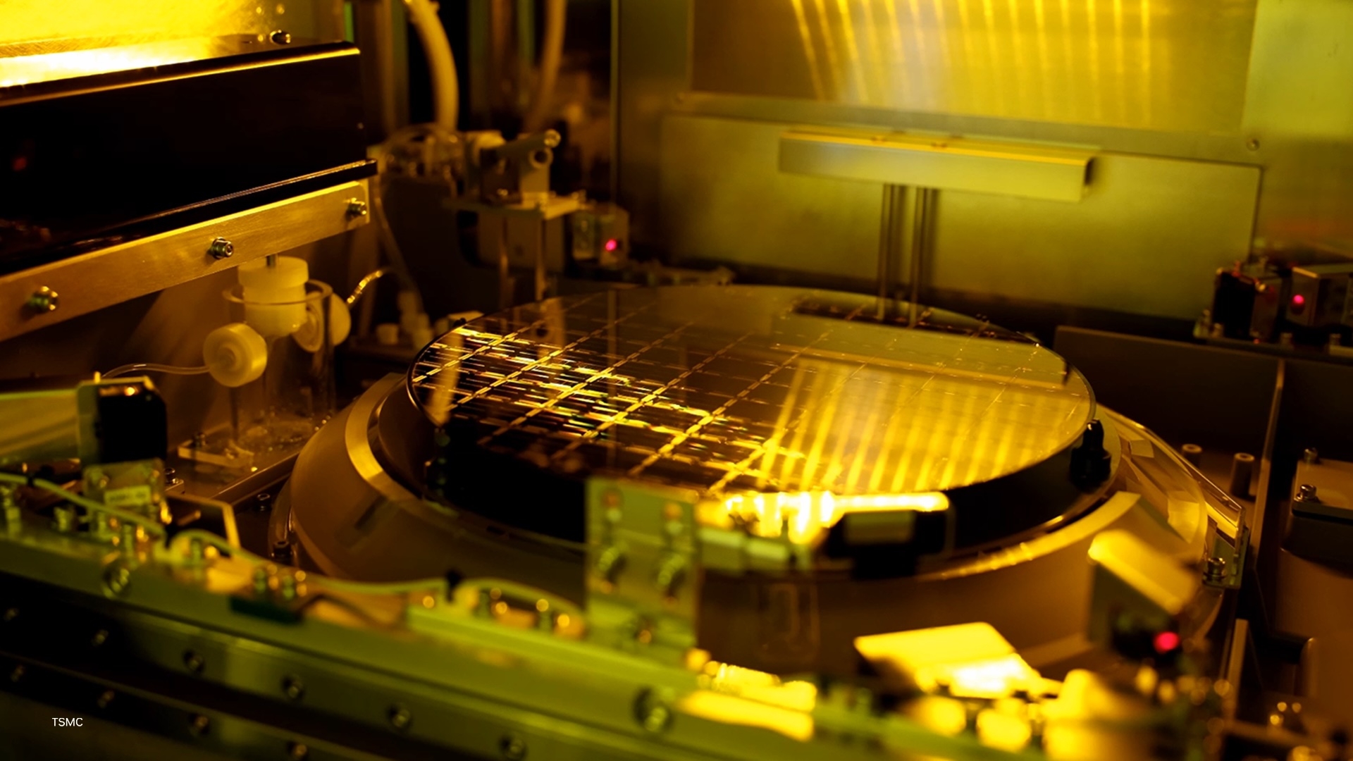
At GTC Taipei on June 1, 2026, NVIDIA and TSMC said they are deepening their collaboration to embed AI directly into chip design and manufacturing. The partnership rolls NVIDIA's CUDA-X libraries, Metropolis vision-AI stack, TAO Toolkit and Omniverse simulation platform into TSMC's lithography, transistor and process simulation, advanced process control, fab operations and yield-management workflows.
CUDA-X and Metropolis on the fab floor
TSMC is using NVIDIA-accelerated computing to shrink simulation cycles for new process nodes — work that today can run for weeks across thousands of CPU cores. Metropolis and the NVIDIA TAO Toolkit are being applied to automated defect inspection with vision AI, improving detection of nanometer-scale defects while cutting the labeling and retraining burden that has historically made vision systems brittle as process recipes evolve.
FabTwin: an Omniverse digital twin of the fab
The most ambitious piece is FabTwin, a virtual fab environment TSMC is building with NVIDIA Omniverse libraries. FabTwin lets engineers evaluate process-tool layouts, contamination flows and material-handling robot routing digitally before any physical change to a fab. By testing complex configurations in simulation first, TSMC can compare more options in parallel and surface constraints — bottlenecks at lithography clusters, AMHS conflicts, utility ceilings — before they appear on a live floor.
Why this matters for the AI buildout
TSMC's leading-edge nodes underpin almost every major AI accelerator — including NVIDIA's own Blackwell line and the new Crescent Island AI inference platforms shipping into hyperscalers. Anything that compresses TSMC's time-to-yield or tightens defect rates translates directly into more accelerators per wafer and faster ramps on next-generation processes. For NVIDIA, embedding its software stack inside TSMC also closes the loop on a 'design with AI, manufacture with AI' message that Jensen Huang has been pushing since GTC.
What's new versus past collaboration
NVIDIA and TSMC have worked together on EDA and computational lithography acceleration for years. The 2026 announcement marks the broadest disclosed integration so far — moving from point tools (faster OPC, faster Monte Carlo defect simulation) into fab-wide operational systems, including digital twins of physical tool layouts. It also commits TSMC to NVIDIA's Omniverse stack, an important reference win against Siemens, Cadence and Synopsys digital-twin offerings.
Industry context
The announcement landed alongside NVIDIA's new RTX Spark Superchip for AI PCs (also manufactured on TSMC's 3-nanometer family) and follows a wave of NVIDIA partnerships including humanoid robotics deployments with Apptronik and the GR00T reference humanoid with Unitree. Together they sketch a stack in which NVIDIA software touches the chip from logic synthesis through factory floor to embodied deployment.
Reporting based on coverage from NVIDIA Newsroom, GlobeNewswire, HPCwire and Stockhouse.